个人资料
教育经历
2006年至今
承担南开大学材料化学和分子生物专业本科生A类课程《大学物理基础》,每年学生人数120左右
工作经历
1998年9月-2000年8月 中国科学院物理研究所,北京, 博士后, 合作导师:周均铭研究员
研究方向:分子束外延GaAs量子阱微腔、垂直腔面发射激光器、量子阱光折变材料。具体指导博士生三名研究光折变器件,激光器和硅基光学非线性材料
2000年9月-2001年9月 日本东京大学工学部电子工程系,JST博士后,日本科技振业集团资助, 合作导师:田中雅明 (Masaaki Tanaka)教授,研究方向:Mn掺杂III-V族GaMnAs 稀磁半导体薄膜材料分子束外延和磁光特性
2000年10月-2006年9月Rossendof研究中心离子束物理和材料研究所,Dresden,德国,博士后,合作导师:Manfred Helm 教授, Wolfgang Skorupa 博士
研究方向:高效率硅基电致发光器件和电光调制器件
具体指导两名博士生研究硅pn结半导体微腔LED和稀土掺杂硅MOS发光器件。
2006年至今南开大学物理学院和泰达应用物理学院, 教授,博士生导师,研究方向:硅基光子学与储能器件
个人简介
1991年毕业于吉林大学物理系,同年考入长春物理所,先后在中科院物理所、日本东京大学、德国Rossendorf研究中心工作,现任南开大学教授。从事硅基电致发光研究20余年,分别在离子注入的硅pn结LED、Er掺杂纳米硅、稀土离子注入的SiO2 MOS结构三种国际前沿的硅基电致发光器件研究方面取得了较大的进展。曾荣获德国Rossendorf研究中心2004年度的先进科研奖励。《Laser Focus World》和《Science Daily》曾刊登专题的文章,介绍了他在高效率紫外和波长从红到蓝可调的硅基发光器件的工作。2006年回国工作,创建了南开大学硅光子学与储能器件实验室。目前在国内外核心期刊发表论文80余篇。现任中国发光学会和中国掺杂纳米材料发光会议委员。
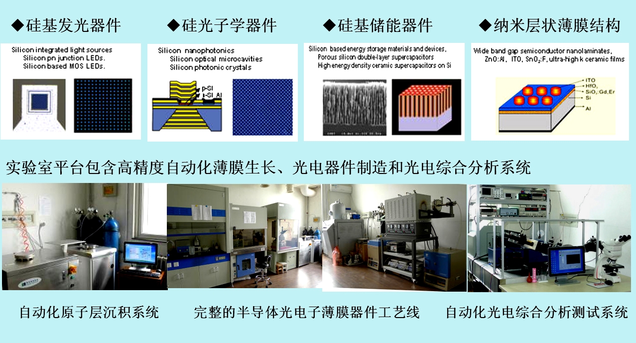
研究领域硅光子学与储能器件实验室 硅光子学与储能器件实验室留学回国人员 实验室遵循材料科学研究规律,吸收德国科研机构高效精确的科学理念,配备了两套自动化原子层沉积系统,使得纳米复合材料制备可精确到单原子层尺度。实验室包含一条完整的薄膜光电子原型器件制造工艺线,一套自动化的光电器件综合分析测试系统,可自主完成包括材料生长、器件制备到发光光谱学、光学和电学特性分析测试的一整套研究进程。实验室的主要设备和测试系统均根据可重复性实验要求进行改造,并开发了配套的自动控制程序,可以把研究人员从大量繁琐的重复工作中解脱出来,以便专心构思研究方向,设计独特的材料和器件结构,取得具有自主知识产权的研究成果。
实验室按照国际先进实验室的标准培养研究生,特别适合于立志科学,具有自主创新意识和独立工作能力的青年人从事研究工作。高效精准的研究平台可以支撑多种精细材料和微纳结构器件的研究工作,取得高水平创新性研究成果。实验室已经与德国、瑞典、意大利、英国、美国等国的研究机构建立了广泛合作与联系。希望出国深造的学生可以预先学到与国际先进实验室接轨的研究方法和科研技能。 具备高尚科学道德,具备独立从事科学研究工作能力是实验室一贯坚持的人才培养目标。能够完成严格的科学研究训练的毕业生自然具备信息查询整理能力、课题规划能力、执行能力、中英文写作能力、中英文报告能力等高水平专业人才的基本素质。实验室还提供广泛的专业技术学习环境,涵盖机械设计与加工技术、复合材料设计、现代薄膜沉积技术、光刻技术、半导体工艺、光谱测量技术、光电测试技术、材料结构和组分分析、自动化控制编程等综合研发技能训练,合格的毕业生可以成为半导体芯片、太阳能光伏、LED照明、液晶显示、光通讯、超级电容等信息和能源企业、大专院校和研究机构急需的专业技术人才。 硅基发光材料和器件 硅为间接带半导体材料,发光效率很低,获得效率高并且能与CMOS工艺兼容的硅电致发光器件一直是半导体光电子领域的一个难题,也是制约硅半导体集成光子学发展的瓶颈,因此硅基光源的研究对下一代半导体技术的发展具有重要的意义。 实验室近年来分别在离子注入的硅pn结LED、Er掺杂纳米硅、稀土离子注入的SiO2 MOS结构硅基电致发光器件研究方面取得了重要进展,处于国际领先水平。 在以前工作的基础上,我们采用新技术从原子层面人工设计和制备硅基电致发光器件。主要用原子层沉积原位生长稀土掺杂的SiO2层状发光薄膜,通过对薄膜掺杂组分进行精细调控减少缺陷,调控过热电子的输运过程和发光中心周围的晶体长环境。进一步提高稀土掺杂MOS结构电致发光器件的效率和稳定性。 硅发光方向先后获得两项国家自然科学基金,一项973项目,一项教育部新世纪人才项目,回国留学人员基金、南开大学引进人才启动项目等7个国家和部级项目,从2006年起累计获得经费249万元。 High-k微电子材料 随着集成电路工艺向更小尺度推进,场效应晶体管的尺寸不断减小,SiO2栅层的厚度要相应的减小到2纳米以下,电子从硅衬底隧穿到栅电极中,从而引起巨大的漏电电流,使得半导体器件过热而无法正常工作的。要减小漏电流,就必须寻找一种介电常数比SiO2更高的high-k材料,从而使物理厚度更厚的high-k材料产生与SiO2相同的电容值,进而避免电子隧穿效应的产生,目前intel公司45纳米工艺以下的处理器全部采用high-k栅介质层。 目前我们实验室利用原子层沉积技术成功生长出HfO2 、Al2O3高介电常数薄膜材料。我们将把这些薄膜应用在复合薄膜硅MOS 电致发光器件上, 提高器件性能。介电常数高达104 的巨介电常数材料如钙钛矿型氧化物陶瓷材料材料是固态高能量存储密度的超级电容器的核心介质材料,我们正在利用原子层沉积方法研制巨介电薄膜材料,主要研究四元组分钙钛矿型氧化物陶瓷材料的高介电常数机理、原子层配比生长、结晶控制、以及介电损耗和漏电流抑制问题。 宽禁带半导体透明导电薄膜 可见光透明导电薄膜在太阳能电池,导电玻璃和显示器件方面具有广泛的应用价值。目前我们利用二乙基锌和水作为前驱体体成功生长出ZnO:Al透明导电薄膜,其在可见光区透过率在90%,薄膜电阻率在E-3欧姆厘米。同时我们还可以生长ITO和SnO2:F透明导电薄膜。 硅超级电容储能器件 超级电容是一种容量在法拉量级的大容量电容器,以干净的方式存储电能,具有大电流充放电和近乎无限的循环次数。超级电容器如果完全替代蓄电池,在全球将会拥有超过1000亿美元的市场价值。目前商品化的超级电容器主要为活性炭、碳纤维布和金属氧化物电极,比电容最高仅为 多孔硅材料孔隙率与活性炭相当,通过在氢氟酸溶液中阳极氧化腐蚀就可获得,空隙率和孔洞大小可以精确控制。多孔硅超级电容理论上容质比率可达到
教学工作2006年至今 承担南开大学材料化学和分子生物专业本科生A类课程《大学物理基础》, 每年学生人数120左右 科研项目
论文著作Publications (2014) 85 Strong electroluminescence from SiO2-Tb2O3-Al2O3 mixed layers fabricated by atomic layer deposition L. Rebohle, M. Braun, R. Wutzler, B. Liu, J.M. Sun, M. Helm, W. Skorupa Appl. Phys. Lett. 104, 251113 (2014). http://dx.doi.org/10.1063/1.4885418 84 Rare Earth Doped Metal-Oxide-Semiconductor Structures: A Promising Material System or a Dead End of Optoelectronic Evolution? L. Rebohle, Y. Berencén, M. Braun, B. Garrido, D. Hiller, B. Liu, J. M. Ramírez, J. M. Sun, R. Wutzler, M. Helm and W. Skorupa, ECS Trans. 2014 61 (5): 175-185 . Publications (2013) 83.Electrical and optical properties of Al-doped ZnO and ZnAl2O4 films prepared by atomic layer deposition, Qiongqiong Hou, Fanjie Meng and Jiaming Sun* Nanoscale Research Letters 8: 144-(2013), doi:10.1186/1556-276X-8-14428 March 2013 (SCI) Publications (2012) 82.Highly efficient silicon light emitting diodes produced by doping engineering,(综述) Jianming SUN, M. HELM, W. SKORUPA, B. SCHMIDT, A. MÜCKLICH,Frontiers of Optoelectronics,5(1):7-12 (2012). 84.The observation of the localized surface plasmons and its coupling, Junmei Li, Xiaoxuan Xu, Yufang Wang, Meng Wang, Zhifu Dong, Wanhui Tian, Jiaming Sun, Cunzhou Zhang and Bin Wang*,J. Raman Spectrosc. 43, 863–868(2012)(SCI) Publications (2011) 83.Preparation of Tetrapod-Like Nanostructure Array and Used as the Surface-Enhanced Raman Scattering Substrates, Li、 Junmei、 Xu、 Xiaoxuan、 Wang、 Yufang、 *Wang、 Bin、 Wang、 Meng、 Tian、 Wanhui、 Dong、 Zhifu、 Sun、 Jiaming、 Zhang、 Cunzhou, Journal of Nanoscience and Nanotechnology, 11(10), pp 8576-8579, (2011)(SCI) 82.A Novel Method for Fabricating the Surface-Enhanced Raman Scattering Substrates and Its Enhanced Properties,Li、 Junmei、*Xu、 Xiaoxuan、 Wang、 Bin、 Wang、 Yufang、 Wang、 Lin、 Zhang、 Cunzhou、 Sun、 Jiaming,Journal of Nanoscience and Nanotechnology, 10(11), pp 7774-7777, 2010/11(SCI) 81.Er 离子注入的富硅SiO2 MOS-LED的可见和红外电致发光特性,刘海旭,孙甲明*,孟凡杰,侯琼琼,发光学报,32(8), 752-753(2011). 80.Nanosecond field-induced quenching of the luminescence from Er-doped silicon nanocrystals H. X. Liu, F. J. Meng, J. M. Sun, Journal of Nanoscience and Nanotechnology,11, 1-3 (2011).(SCI) Publications (2010) 79.Silicon-based light emission in ultraviolet J. M. Sun, S. Prucnal, A. Mücklich, W. Skorupa, and M. Helm, 2010 7th IEEE International Conference on Group IV Photonics Beijing China(GFP 2010) p 338-40 (2010)(SCI) 78.A Novel Method for Fabricating the Surface-Enhanced Raman Scattering Substrates and Its Enhanced Properties, Li JM (Li, Junmei)1, Xu XX (Xu, Xiaoxuan)1,2, Wang B (Wang, Bin)1,2, Wang YF (Wang, Yufang)1, Wang L (Wang, Lin)1, Zhang CZ (Zhang, Cunzhou)1, Sun JM (Sun, Jiaming)1 JOURNAL OF NANOSCIENCE AND NANOTECHNOLOGY , 10 (11), 7774-7777(2010). (SCI) 77.以PAA为模板制备SERS基底及对三聚氰胺的检测, Using PAA Template to Fabricate SERS Substrate and the SERS Detection of Melamine, 李俊梅; 徐晓轩; 王玉芳; 王斌; 孙甲明; 张存洲, 光谱学与光谱分析.30(10), P2663-2664 (2010). 76. Physical limitations of the electroluminescence mechanism in terbium-based light emitters: Matrix and layer thickness dependence,Rebohle, L. Lehmann, J.; Prucnal, S.; Sun, J.M.; Helm, M.; Skorupa, W. Applied Physics B: Lasers and Optics, v 98, n 2-3, p 439-442, February 2010. (SCI) Publications (2009) 75.半绝缘Si/SiO2 超晶格结构在交流电场下的电致发光特性,张新霞,孙甲明,张俊杰,杨 阳,刘海旭,《材料科学与工程学报》27,129-131(2009)。 74.纳米硅微晶对于Er离子掺杂的SiO2薄膜的光致发光和电致发光的不同影响,张俊杰,孙甲明,杨 阳,张新霞,刘海旭,W. Skorupa,M. Helm,《材料科学与工程学报》27,135-138(2009)。 73.离子注入缺陷局域掺杂的高效率硅pn结发光二极管, 杨 阳,孙甲明,张俊杰,张新霞,刘海旭,W. Skorupa,M. Helm, 《材料科学与工程学报》27(1),142-145(2009)。 72.稀土离子注入的高效率硅基纳米材料电致发光器件,孙甲明,刘海旭,张俊杰,杨 阳,张新霞,W. Skorupa,M. Helm,《材料科学与工程学报》27(1), 121-4(2009)。 71. Light emissionfrom ion-implanted silicon J. M. Sun, M. Helm1, W. Skorupa, B. Schmidt, and A. Mücklich,Phys. Status Solidi C 6, No. 3, 716– 720 (2009) (SCI) Publications (2008) 70. Energy transfer from Gd to Er atoms in SiO2(GdEr)-MOSLEDs produced by ion implantation S.Prucnal, J. M. Sun, L.Rebohle, and W.Skorupa, Materials Science and Engineering B 146, 241-244 (2008)(SCI) 69.Giant stability enhancement of rare-earth implanted SiO2 light emitting devices by an additional SiON protection layer J. M. Sun, L. Rebohle, S. Prucnal, M. Helm, and W. Skorupa, Appl. Phys. Lett. 92, 071103 (2008). (SCI) Publications (2007) 68 Quenching of electroluminescence and charge trapping in high-efficiency Ge-implanted MOS light-emitting silicon diodes AN. Nazarov, I.N Osiyuk, J.M. Sun, R.A. Yankov, W. Skorupa, I.P. Tyagulskii, V.S. Lysenko, S. Prucnal, T. Gebel, and L. Rebohle, APPLIED PHYSICS B 87, 129-134 (2007). (SCI) 67.Correlation between defect-related electroluminescence and charge trapping in Gd-implanted SiO2 layers Prucnal, S; Sun, JM; Nazarov, A; Tjagulskii, IP; APPLIED PHYSICS B-LASERS AND OPTICS 88, 241-244 (2007) (SCI) 66.Electronegativity and point defect formation in the ion implanted SiO2 layers S. Prucnal, J.M Sun, H. Reuther, C. Buchal, J. Zuk,; W. Skorupa, Vacuum 81, 1296-1300 (2007). (SCI) 65. Silicon-based light emitter has luminescent middle layer between contacts with additional dielectric protective layers on its boundaries with these layers Patent Number(s): DE102005052582-A1 Assignee(s): NANOPARC GMBH Inventor(s): REBOHLE L; GEBEL T; SKORUPA W; SUN J 64. Fourfold increase of the ultraviolet (314 nm) electroluminescence from SiO2:Gd layers by fluorine coimplantation and flash lamp annealing, Appl. Phys. Lett. 91, 181107 (2007)(SCI) 63. InP同质外延的不稳定生长:小丘的形成 皮 彪 , 孙甲明 , 林耀望 , 姚江宏 ,邢晓东 , 蔡 莹 , 舒 强 , 贾国治 , 刘如彬, 李 丹, 王占国 (Unstable Growth in InP Homoepitaxy: Mound Forma tion, Pi Biao , Sun Jiam ing , Lin Yaowang , Yao Jiang hong , X ing Xiaodon , Cai Ying , Shu Qiang, Jia Guozhi ,Liu Rubin , L i Dan ,Wang Zhanguo, ) 人工晶体学报, 36 (2), 263-266 (2007). 62. Morphological and electrical properties of InP grown by solid source molecular beam epitaxy, Biao Pi, Yongchun Shu, Yaowang Lin, Jiaming Sun, Shengchun Qu, Jianghong Yao, Xiaodong Xing, Bo Xu, Qiang Shu, Zhanguo Wang, Jingjun Xu,Journal of Crystal Growth 299, 243–247 (2007). (SCI) 61. Switchable two-color electroluminescence based on a Si metaloxide-semiconductor structure doped with Eu S. Prucnal, J. M. Sun, 60. Strong Improvement of the Electroluminescence Stability of SiO2:Gd Layers by Potassium Co-implantation S. Prucnal, J. M. Sun, H. Reuther, W. Skorupa, and Ch. Buchal ,Electrochem. Solid-State Lett. 10, J30 (2007). ( SCI) 59. Flash Lamp Annealing vs Rapid Thermal and Furnace Annealing for Optimized Metal-Oxide-Silicon-Based Light-Emitting Diodes, S. Prucnal, J. M. Sun, A. Muecklich, and W. Skorupa , Electrochem. Solid-State Lett. 10, H50 (2007). (SCI) . Publications (2006 ) 58. Silicon-on-insulator microcavity light emitting diodes with two Si/SiO2 Bragg reflectors , (SCI) J. Potfajova, J.M. Sun, B. Schmidt, T. Dekorsy, 57. Charge trapping phenomena in high-efficiency metal-oxide-silicon light-emitting diodes with ion-implanted oxide, A. Nazarov,_, I. Osiyuka,, I. Tyagulskii, V. Lysenko, S. Prucnal, J. Sun, W. Skorup, R.A. Yankov, Journal of Luminescence 121, 213–216 (2006). (SCI) 56. Traditional hot-electron MOS devices for novel optoelectronic applications T. Dekorsy, J. Sun, W. Skorupa, M. Helm, L. Rebohle, and T. Gebel, Springer Proceedings in Physics vol. 110, 265 (2006) (SCI) 55. Increase of blue electroluminescence from Ce-doped SiO2 layers through sensitization by Gd3+ ions J. M. Sun, S. Prucnal, W. Skorupa, M. Helm, L. Rebohle, and T. Gebel, Appl. Phys. Lett. 89, 091908 (2006). (SCI) 54. Electroluminescence properties of the Gd3+ ultraviolet luminescent centers in SiO2 gate oxide layers J. M. Sun, S. Prucnal, W. Skorupa, T. Dekorsy, A. Mücklich, M. Helm, L. Rebohle, and T.Gebel, J. Appl. Phys. 99, 103102 (2006). (SCI) Publications (2005) 53. Rare earth ion implantation for silicon based light emission, W. Skorupa, J.M. Sun, S. Prucnal, L. Rebohle, T. Gebel, A.N. Nazarov, I.N. Osiyuk, and M. Helm, Gettering and defect engineering in semiconductor technology XI, Solid State Phenomena 108-109, 755-760 (2005) .(SCI) 52. Efficient silicon based light emitters M. Helm, J.M. Sun, J. Potfajova, T. Dekorsy, B. Schmidt, and W. Skorupa, 4th Workshop on Semiconductor Nanodevices and Nanostructured Materials, MAR 09-13, 2005, Microelectronics Journal 36, 957 (2005). (SCI) 51. Bright green electroluminescence from Tb3+ in silicon metal-oxide-semiconductor devices J. M. Sun, W. Skorupa, T. Dekorsy , and M. Helm, J. Appl. Phys. 97, 123513 (2005). (SCI) 50. Efficient silicon light emitting diodes by boron implantation: the mechanism, J.M. Sun , T. Dekorsy, W. Skorupa, A.Muecklich, B. Schmidt, M. Helm, Optical Materials 27, 1041–1045 (2005). (SCI) 49. On the mechanism of electroluminescence excitation in Er-doped SiO2 containing silicon nanoclusters J.M. Sun, W. Skorupa, T. Dekorsy, M. Helm, A.N. Nazarov, Optical Materials 27, 1050–1054 (2005). (SCI) 48. Efficient electroluminescence from rare-earth implanted SiO2 metal-oxide-semiconductor structures. J.M.Sun, W.Skorupa, T.Dekorsy, and M.Helm, 2005 2nd IEEE International Conference on Group IV Photonics, Antwerp, Belgium, 21-23 Sept. 2005. 2005 2nd IEEE International Conference on Group IV Photonics (IEEE Cat. No. 05EX1053) : 48-50 (2005). (SCI) 47. Origin of efficient light emission from Si pn diodes prepared by ion implantation. T. Dekorsy, J. M. Sun, W. Skorupa, A. Mücklich, B. Schmidt, and M. Helm, AIP Conf. Proc.772, 1539 (2005). (SCI) 46. Photoluminescence of Er-doped SiO2 layers containing Si nanoclusters using dual ion implantation and annealing X.Q. Cheng, J.M. Sun, R. Kögler, W. Skorupa, W. Möller and S. Prucnal, Vacuum, 78, 667 (2005). (SCI) 45.Optical and microstructural properties of doubly Ge–Si implanted SiO2 layers S. Prucnal, X.Q. Cheng, J.M. Sun, R. Kögler, J. Żuk and W. Skorupa, Vacuum 78, 693 (2005). (SCI) 44. Light emission and charge trapping in Er-doped silicon dioxide films containing silicon nanocrystals, A. Nazarov, J.M. Sun, I. N. Osiyuk, I. P. Tjagulskii, V. S. Lysenko, W. Skorupa, R.A. Yankov , and T. Gebel Appl. Phys. Lett. 86, 151914 (2005). (SCI) 43.Efficient light emitting diodes based on nanoscale silicon, M. Helm, J. Sun, J. Potfajova, S.Winnerl, T. Dekorsy, W. Skorupa, B. Schmidt, A. Mücklich, International Conference on Superlattices, Nano-Structures and Nano-Devices, JUL 19-23, 2004, Physica Status Solidi C 2, 2941 (2005). (SCI) Publications (2004 ) 42. Efficient ultraviolet electroluminescence from a Gd-implanted silicon metal–oxide–semiconductor device J. M. Sun, W. Skorupa, T. Dekorsy, and M. Helm, Appl. Phys. Lett. 85, 3387 (2004). (SCI) 41. Below-band-gap electroluminescence related to doping spikes in boron-implanted silicon pn diodes, J. M. Sun, T. Dekorsy, W. Skorupa, B. Schmidt, A. Mücklich, and M. Helm, Phys. Rev. B 70, 155316 (2004). (SCI) 40. Silicon-based electrically driven microcavity LED, J. Potfajova, J.M. Sun, S. Winnerl, T. Dekorsy, W. Skorupa, B. Schmidt, M. Helm, S. Mantl and U. Breuer, Electronic Letters 40, 904 (2004). (SCI) 39. Light-emitting silicon pn diodes (invited) T. Dekorsy, J.M. Sun, W. Skorupa, B. Schmidt, M. Helm, Appl. Phys. A 78, 471 (2004). (SCI) 38. Ion Beam Processing for Silicon - Based Light Emission (invited) W. Skorupa, T.Dekorsy, T. Gebel, M. Helm, , V.S. Lysenko, , A.N. Nazarov, , I.N. Osiyuk, , L. Rebohle, B. Schmidt, and J.M. Sun, Symposium on Radiation Effects and Ion-Beam Processing of Materials held at the 2003 MRS Fall Meeting, DEC 01-05, 2003, Mat. Res. Soc. Symp. Proc.792, 357-368 (2004). (SCI) Publications (2003) 37.Electroluminescence from thin SiO2 layers after Si- and C-coimplantation, T. Gebel, L. Rebohle, J. Sun, W. Skorupa, Physica E 16, 366 (2003). (SCI) 36. Correlation of charge trapping and electroluminescence in highly efficient Si-based light emitters, T. Gebel, L. Rebohle, J. Sun, W. Skorupa, A.N. Nazarov, I. Osiyuk, Physica E 16 499(2003). (SCI) 35. Origin of anomalous temperature dependence and high efficiency of silicon light-emitting diodes J. M. Sun, T. Dekorsy, W. Skorupa, B. Schmidt, and M. Helm, Appl. Phys. Lett. 83, 3885 (2003). (SCI) 34. Bound-exciton-induced current bistability in a silicon light-emitting diode, J. M. Sun, T. Dekorsy, W. Skorupa, B. Schmidt, and M. Helm, Appl. Phys. Lett. 82, 2823 (2003). (SCI) Publications (1997-2001) 33. Strong room-temperature exciton-photon coupling in low-finesse microcavities grown by molecular-beam epitaxy, J..M. Sun, Y.F. Zhang, Y, J. Han, W.X. Wang, C.L. Bao, W. Li, J. M. Zhou, Q. Huang, B. H. Feng and X. L. Zhang, J. Crystal Growth 227, 138 (2001). (SCI) 32. Strong room-temperature exciton-photon coupling in low-finesse microcavities entirely filled with GaAs/AlGaAs quantum wells J. M. Sun, Y.F. Zhang, W.X.Wang, C.L. Bao, W.Li, J.M. Zhou, Qi Huang. 7th international conference on Molecular Beam Epitaxy, 31. Two-wave mixing in Stark geometry photorefractive quantum wells under a magnetic field, Y. F. Zhang, J. M. Sun, M. H. Zhang, Z. G. Zhang, Q. Huang, Appl. Phys. Lett. 76, 2185 (2000). (SCI) 30. Photoluminescence characterization of Si-doped low-emperature grown GaAs and GaAs/AlGaAs multiple quantum wells, M.H.Zhang, Y.F.Zhang, Q.Huang, C.L.Bao, J.M.Sun, J.M.Zhou, J.Crystal.Growth, 209,37(2000). (SCI) 29. Optimum incident light intensity in stark geometry photorefractive multiple quantum wells device, Y.F.Zhang, M.H.Zhang, J.M.Sun Z.G.Zhang, Q.Huang, J.M.Zhou, Eleventh International Conference on Molecular Beam Epitaxy, 28. Two-wave mixing in stark geometry photorefractive quantum wells under a magnetic field, Y.F.Zhang, J.M.Sun, M.H.Zhang, Z.G.Zhang, Q.Huang, and J.M.Zhou SPIE's International Symposium "ISPA’99" 27. High-frequency electric modulation of stark geometry multi-quantum wells photorefractive device, Y.F.Zhang, J.M.Sun, Q.Huang, J.M.Zhou, SPIE’s Symposium on Integrated Optoelectronics, 26. The mechanism of the degradation of photorefractive effect in low-temperature grown GaAs/AlGaAs multiple M.H.Zhang, Y.F.Zhang, J.M.Sun, Q.Huang, J.M.Zhou quantum wells, SPIE's International Symposium "ISPA’99" , Beijing, China. 25. Influence of the excess As on the optical properties of GaMnAs films grown by low-temperature molecular beam epitaxy. J.M.Sun, A.M. Nazmul. H.Shimizu, S. Ohya, and M. Tanaka, Extend abstracts of the 20th EMS, 24. Third-order optical nonlinear properties of amorphous Si/SiO2 superlattices fabricated by magnetron sputtering, N. N. Liu, J.M.Sun, S.H. Pan, Z.H. Chen, W.S. Shi, R. P. Wang, and X.G.Wang, Optics Communications, 176, 239-243, 2000. (SCI) 23. Optical properties of amorphous Si/SiO2 superlattices N. N. Liu, J. M. Sun, S.H. Pan, Z. H. Chen, R.P. Wang, W.S. Shi and X.G. Wang Superlattices and Microstructures 28, 157 (2000). 22. Photoluminescence from amorphous Si/SiO2 superlattices fabricated by magnetron sputtering, Ning-ning Liu, Jia-ming Sun, Shao-hua Pan, Zheng-hao Chen, Rong-ping Wang, and Wen-sheng Shi, The fifth IUMRS international conference on advanced materials, 21. Raman scattering and photoluminescence studies on Si/SiO[sub 2] superlattices M. Benyoucef, M. Kuball, J. M. Sun, G. Z. Zhong, and X. W. Fan, J. Appl. Phys. 89, 7903 (2001). (SCI) 20. Electroluminescence from ITO/SiO2/Ta2O5/Al multiple-layer structure excited by hot electrons J. M. Sun, G.Z. Zhong, X. W. Fan , G. Z. Fu and C. W. Zheng, J. Non-Crystalline Solids 212 ,192 ( 1997). (SCI) 19. Electroluminescence from CaS:TmF3 film prepared by radio frequency magnetron reactive sputtering J. M. Sun, G. Z. Zhong, X. W. Fan , G. Z. Fu and C. W. Zheng, Gerd O. Mueller and Regina Mueller-Mach, J. Appl. Phys. 83(6), 3374 ( 1998). 中文期刊 18.非对称F-P腔反射式半导体量子阱光折变器件的生长与性能研究, 孙甲明,张燕锋,张满红,黄绮,周均铭。第五届全国分子束外延学术会议,昆明。 17.衬底取向对低温生长的GaAs/AlGaAs光折变多量子阱中的缺陷的光学性质的影响, 张满红,张燕锋,孙甲明,黄绮,周均铭第五届全国分子束外延学术会议,昆明。 16.新型垂直场光折变器件的研制,张燕锋,孙甲明,张满红,黄绮,周均铭 第五届全国分子束外延学术会议,昆明。 15. 非晶Si/SiO2超晶格的制备及其光谱研究, 刘宁宁,孙甲明,潘少华,陈正豪,王荣平,师文生,王晓光,中国科学 49, R1019(2000)。 14. Si/SiO2超晶格的非线性光学性质,刘宁宁,孙甲明,潘少华,陈正豪,王荣平,师文生,王晓光, 陈凡,49,科学通报, 45, 2383(2000)。 13. 含GaAs/AlGaAs多量子阱的半导体微腔的光折变效应的研究 孙甲明,张燕峰,张满红,周均铭和黄绮第五界全国分子束外延会议,云南,昆明,1999 12.含纳米硅微粒的富硅二氧化硅的蓝色薄膜交流电致发光 孙甲明钟国柱 范希武 李长华 1998年第八届全国发光学会议文集 11. 探测非晶SiO2加速层中热电子能量分布变化的新方法 孙甲明 钟国柱 范希武 李长华1998年第八届全国发光学会议文集 10. 衬底温度对电子束蒸发CaS:TbF3薄膜电致发光亮度的影响 孙甲明钟国柱 范希武 郑陈玮 《发光学报》19(1),36 (1998)。 9. 射频磁控溅射CaS:TmF3 薄膜的电致发光及其激发过程的研究 孙甲明钟国柱 范希武 郑陈玮《发光学报》19(1),31 (1998) 8. CaS:TmF3粉末发光材料的制备 孙甲明钟国柱范希武郑陈玮《无机材料学报》 6, 350, (1998) 7 复合绝缘层交流薄膜电致发光显示屏的综合设计 孙甲明钟国柱 付国柱 郑陈玮 张曙芝 范希武《发光学报》17(3),191(1996)。 6.用MOCVD方法制备的ZnS薄膜的结晶性研究 赵丽娟, 钟国柱, 杨宝钧, 郑陈玮,孙甲明. 光电子·激光, 6, 增刊, 183(1995) 5. n 型多孔硅激发光谱的研究 孙甲明 张吉英范希武 于宝贵 关中素 《凝聚态光学性质研究进展》第七届全国凝聚态光学性质学术会议文集 (1994年8月21-28日) 张存洲熊光楠张光寅编 南开大学出版社 p43 4. 多孔硅中的蓝色发光谱带 孙甲明范希武 韩力 张吉英 费浩生 车颜龙《发光学报》15(2),122(1994) 3. ZnSe—CdZnSe 多量子阱光双稳器件的研制 孙甲明申德振 范希武 张吉英 吕有明 杨宝均 《发光学报》15(2),172(1994)。 2. ZnSe—ZnS超晶格的通光蚀孔及列阵研究 张吉英 孙甲明 范希武 姜锦秀 陈连春, 《发光学报》14(4),316(1993)。 1. 多孔硅的电荷存贮特性与光电压的滞后衰减 孙甲明 张吉英 申德振 范希武 《发光学报》14(2),206 (1993)。 发明专利 1. II—VI 族半导体和超晶格薄膜GaAs衬底的选择性蚀孔技术 发明人:孙甲明,张吉英 ( 于1997年1月申请国家专利, 申请号: 96122294 见1998年《发明专利公报》第25 期,专利申请公开号:5651。 2. Silizium-basiertes optoelektronisches Bauelement, T. Dekorsy,J. M. Sun, W. Skorupa, B. Schmidt, M. Helm, Deutsche Patentanmeldung DE 103 48 269.5 (2003). 指导研究生情况 2010 硕士学位论文:原子层沉积制备的HfO2高K栅介质材料特性研究, 张俊杰, 南开大学2010/5 硕士学位论文:可控无序对高迁移率二维电子系统输运性质的影响, 杨阳, 南开大学2010/5 硕士学位论文:Opal光子晶体的制备及质子辐射和退火对纳米金刚石颗粒的处理, 张新霞,南开大学, 2010/5 2011 硕士学位论文:溶胶-凝胶法制备Tb3+掺杂的SiO2荧光粉性质研究,姚惠梓,南开大学,2011/6 博士学位论文:有序纳米结构的制备及其表面增强拉曼散射特性的研究,李俊梅,南开大学,2011/6 博士学位论文:掺铒富硅二氧化硅电致发光器件的光电特性研究,刘海旭,南开大学,2011/12 2012 硕士学位论文:利用原子层沉积方法制备硅基MOS器件研究,孟凡杰,南开大学,2012/6 硕士学位论文:超声雾化法制备Er3+掺杂SnO2薄膜结构与性质研究,闫艳花,南开大学,2012/6 2013 硕士学位论文:超声雾化气相沉积生长的Zn1-xMgxO薄膜性质的研究,王肖珩,南开大学,2013/6 硕士学位论文:利用溶胶-凝胶法制备稀土掺杂SiO2发光材料研究,靳亚粉,南开大学,2013/6 硕士学位论文:原子层沉积方法制备稀土Gd掺杂SiO2薄膜电致发光器件,侯琼琼,南开大学,2013/6
学术交流 2003 1.Electroluminescence of silicon pn diode produced by boron implantation Lecture (Conference): Frühjahrstagung des Arbeitskreises Festkörperphysik (AKF) der DPG HL 24.5 Dresden 24.- 28.03.2003. 2. Modulation of the electronic transitions of silicon light-emitting diodes produced by boron implantation. E-MRS 2003 Spring Meeting Strasbourg (France) June 10-14 2003, symposium E-VI.3. 2004 3. Temperature dependence of efficient silicon light-emitting diodes prepared by ion implantation J.M. Sun, T.Dekorsy, W. Skorupa, B. Schmidt, and M. Helm DPG-Spring Meeting of the Division Condensed Matter Physics, HL 4. Efficient silicon light emitting diodes by boron implantation: the mechanism J. M. Sun, T. Dekorsy, W. Skorupa, B. Schmidt, A. Mücklich and M. Helm, E-MRS 2004 Spring Meeting Strasbourg (France), May 24-28, 2004, symposium A1V.2. 5.The mechanism in efficient silicon light-emitting diodes. J. M. Sun, T. Dekorsy, W. Skorupa, B. Schmidt, A. Mücklich and M. Helm, 6. Efficient electroluminescence from Tb-implanted silicon metal-oxyde semiconductor devices, J. M. Sun, W. Skorupa, T. Dekorsy, and M. Helm E-MRS 2004 Spring Meeting Strasbourg (France), May 31-June 3rd, symposium C: 'Rare earth doped photonic materials' C-V.03. 7. Modulation of the 1535 nm photoluminiscence from Er-doped Si-rich silicon dioxide by field-induced quenching J. M. Sun , W. Skorupa, T. Dekorsy and M. Helm E-MRS 2004 Spring Meeting Strasbourg (France), May 31-June 3rd, symposium D: Session IV “ Light emitting Si” D-IV.02. 2005 8.Efficient light emission from silicon pn diodes and MOS structures.(invited) J. M. Sun, W. Skorupa, T. Dekorsy and M. Helm 14th International Conference on Luminescence 2005, 9.Efficient electroluminescence from rare-earth implanted SiO2 metal-oxide-semiconductorstructures. J. M. Sun, W. Skorupa, T. Dekorsy, M. Helm, L.Rebohle and T.Gebel. 2nd International Conference on Group IV Photonics, September 21-23, 2005, ThB3, 2006 10. Recent progress in efficient electroluminescence from slicon-based light emitting devices made by ion beam processing (invited) J. M. Sun, S. Prucnal, W. Skorupa, J.Patfojava, B. Schmidt, A. Mücklich, M. Helm, L.rebohle and T. Gebel, E-MRS 2006 Spring Meeting Nice ( 11. Efficient silicon-based optoelectronics devices , J.M. Sun , Institute of Physics Beijing University , 2007 12. 稀土离子注入的SiO2 MOS结构的高效率电致发光,Efficient electroluminescence devices from rare-earth implanted SiO2 MOS structures (invited ) 孙甲明, W.Skorupa, and S. Prucnal. 第11届全国发光学学术会议, 2007年8月20-25日, 长春。 2008 13. Lignt emission from ion implanted silicon, Jiaming Sun 2008 Sino-German Symposium on silicon optoelectronics 9-14th,June 2008, Hangzhou China, (invited ) 14 孙甲明,刘海旭,张俊杰,杨 阳,张新霞,W. Skorupa,M. Helm, 稀土离子注入的高效率硅基纳米材料电致发光器件,第二届全国掺杂纳米材料发光性质学术会议,珠海 2008-11月23-29日. (邀请报告) 15 孙甲明, ,离子注入高效率硅材料电注入发光器件的进展, 2008第二届硅基光电子材料及器件会议,杭州, 2008年6月12-15日. 16 张新霞,孙甲明,张俊杰,杨 阳,刘海旭, 半绝缘Si/SiO2 超晶格结构在交流电场下的电致发光特性, 2008第二届硅基光电子材料及器件会议,杭州, 2008年6月12-15日. 17 张俊杰,孙甲明,杨 阳1,张新霞,刘海旭,W. Skorupa,M. Helm, 纳米硅微晶对于Er离子掺杂的SiO2薄膜的光致发光和电致发光的不同影响, 2008第二届硅基光电子材料及器件会议,杭州, 2008年6月12-15日. 18 杨 阳,孙甲明,张俊杰,张新霞,刘海旭,W. Skorupa,M. Helm, 离子注入缺陷局域掺杂的高效率硅pn结发光二极管,2008第二届硅基光电子材料及器件会议,杭州, 2008年6月12-15日. 2009 19 2009年硅基光电子材料及器件会议,北京,6月27至30日,口头报告题目 富硅SiOB2B基质中Er和纳米硅耦合发光体系的电场效应,孙甲明 2009年硅基光电子材料及器件学术会议文集P15 2010 20 SiO2电子加速薄膜电致发光器件中过热电子能量的二次增强现象,(口头报告) 王肖珩,刘海旭,张新霞,孙甲明,2010年硅基光电子材料及器件研讨会, 21 富硅氮化硅薄膜及Si/Si3N4超晶格结构的交流电致发光,(口头报告) 刘海旭,王肖珩张新霞孙甲明,2010年硅基光电子材料及器件研讨会, 22 集成硅基发光器件的研究,(邀请报告) 孙甲明,第十三届全国发光学及产业研讨会,2010年11月6-8日,苏州,兼任会议委员 23 Nanosecond field-induced quenching of the luminescence from Er-doped silicon nanocrystals,(邀请报告) 刘海旭,孟繁杰,孙甲明,第三届全国掺杂纳米材料发光性质学术会议,2010年8月10-14日,西安,兼任会议委员 学术成果 |